Front End (FE) and Breakout Board
A modular adapter board for sSDR and dSDR modules with an integrated high-performance RF front-end.
Overview
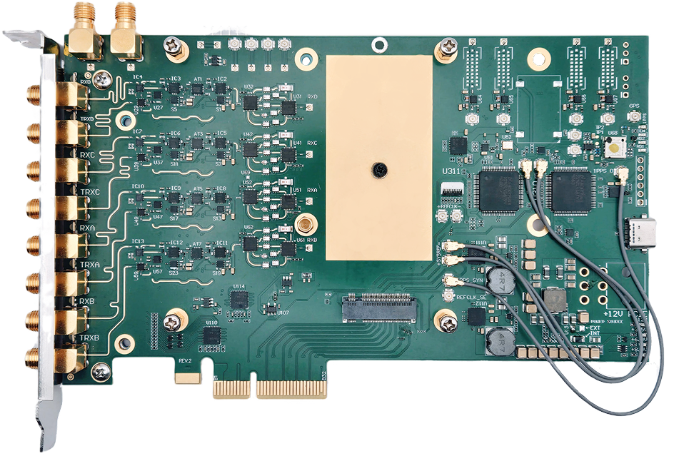
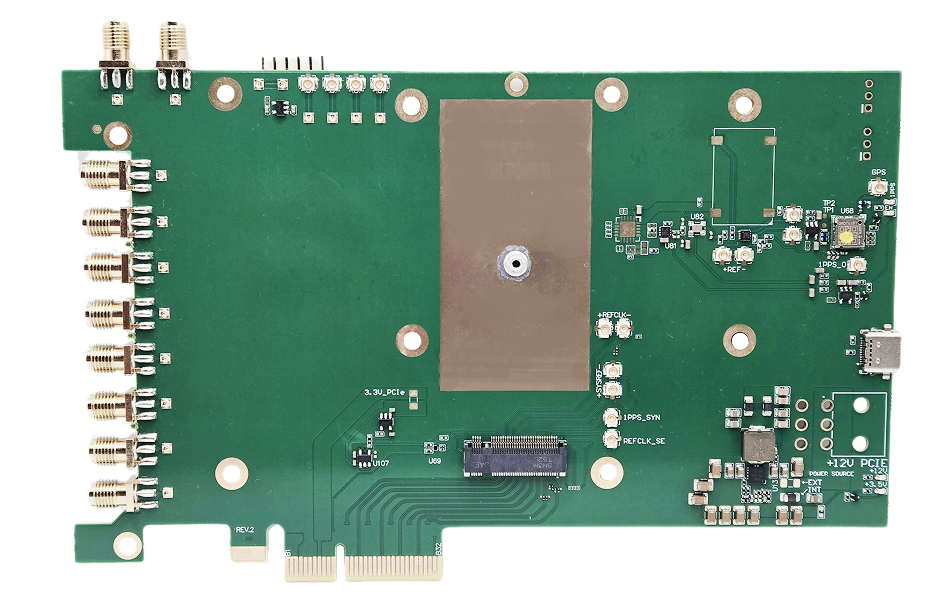
The Front End (FE) is a modular, high-performance adapter board featuring 4 RX and 4 TX channels which can be synchronized. In addition, the board includes fast TX/RX switches for each channel, making it usable for TDD applications.
The board can be used with our dSDR or sSDR transceiver modules.
Breakout board
The Breakout board is the light version of the FE board without the RF front-end components. It is intended for users who want to design their own RF front-end or use the board in a lab environment.
General Specifications
- Clock Synchronization
LMK1C1104
- Module slot
M.2 Key M socket for sSDR or dSDR module
- Form Factor
PCIe x4
RF Specifications
Note
Note
Integrated high-performance RF front-end with low-noise amplifiers, power amplifiers, filters, and switches.
- RF frontend frequency range
50 MHz to 7.2 GHz
- RFIC
- with sSDR module:
LMS7002M + LMS8001
2 RX / 2 TX channels
- with dSDR module:
AFE7900/AFE7901/AFE7950
6 RX / 4 TX channels
- Sample Rate
- with sSDR module:
4 MSps - 100 MSps
- with dSDR module
0.1 MSps - 500 MSps
- Channel Bandwidth
- with sSDR module:
0.5 MHz - 90 MHz
- with dSDR module:
0.5 MHz - 500 MHz
Bifurcation Modes
4×4 MIMO systems
2 independent 2×2 MIMO systems
Target Applications
- Cellular Communication
Enables next-generation 4G/5G wireless networks with high-order massive MIMO and TDD
Fully compatible with Amarisoft and srsRAN
- Directional Finding
Determines the direction of arrival (DoA) of incoming radio signals, enabling precise localization of transmitters
- Beamforming
Focuses on signal transmission and reception in specific directions
Enhances range, improves signal quality, and reduces interference in multi-user environments
Connections
Note
Front side
The front side of the board contains the M.2 socket for the sSDR or sSDR module and 4 MHF7 connectors for RX signals.
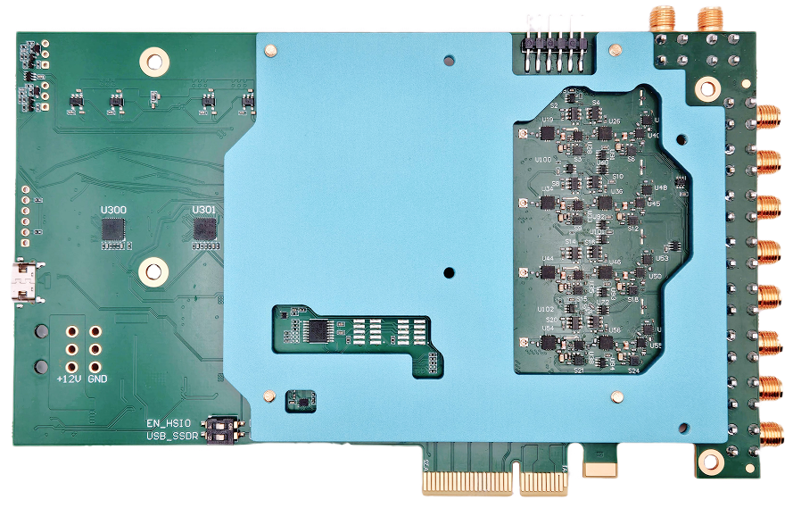
Back side
The front side of the board contains 4 MHF7 connectors for TX signals.
PCI bracket panel
The bracket panel of the FE has 8 external SMA connectors for TX/RX/TRX signals.
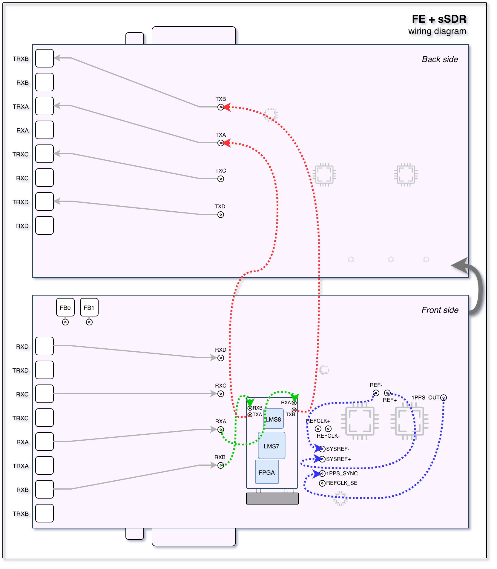
sSDR module connections
The following schematic diagram shows the connections between the FE board and the sSDR module.
dSDR module connections
The following schematic diagram shows the connections between the FE board and the dSDR module.

Breakout board connections
The following schematic diagram shows the connections between the BreakOut board and the dSDR module.

JTAG programming
An installed module(sSDR or dSDR) can be programmed via JTAG using the dedicated 6-pin JTAG header on the FE or BREAKOUT boards.
You can use Digilent HS1 or Digilent HS2 adapters among with openFPGALoader tool for JTAG programming.
Compatible adapters might work, please refer to their documentation for pinout details.
The following image shows how to connect the JTAG adapter to the board properly.
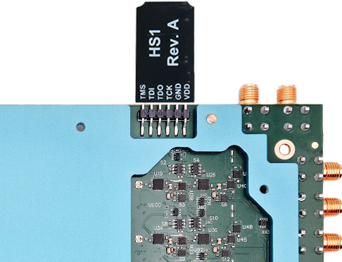
The pinout of the JTAG header is as follows(from left to right):
1 -
TMS- Test Mode Select2 -
TDI- Test Data In3 -
TDO- Test Data Out4 -
TCK- Test Clock5 -
GND- Ground6 -
VDD- Power supply
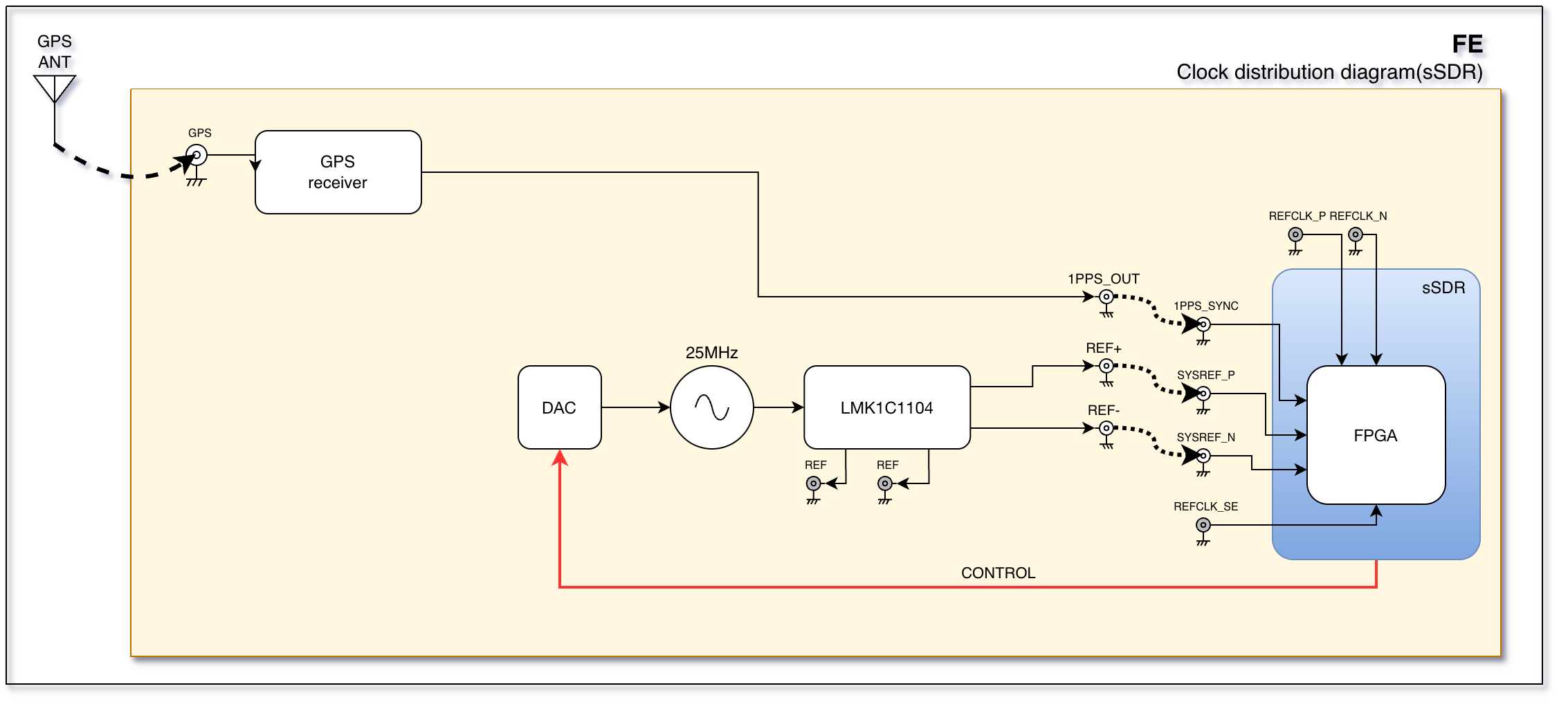
Clocks and synchronization
There are two clock domains on the FE board:
REFCLK: Reference clock used for phase synchronization and RF frequency calibration.
SYSREF: Event synchronization: start, stop, and other control signals.
The FE board can use different clock sources:
On-board crystal oscillator.
GPS synchronization using the on-board GPS module.
sSDR wiring
REF+toSYSREF+.REF-toSYSREF-.1PPS_OUTto1PPS_SYN.
The following diagram shows the clock and synchronization wiring when using the sSDR module.
dSDR wiring
REF+toREFCLK_SE.1PPS_OUTto1PPS_SYN.Connect FPC connector on the FE board(marked as
IOon the schema above) to the FPC connector on the dSDR module.
The following diagram shows the clock and synchronization wiring when using the dSDR module.

RF distribution

Note
sSDR module
For sSDR, the RF distribution should be connected as follows:
RXAtosSDR RX A.RXBtosSDR RX B.TXAtosSDR TX A.TXBtosSDR TX B.
Note
dSDR module
For dSDR, the RF distribution should be connected as follows:
RXAtodSDR RX A.RXBtodSDR RX B.RXCtodSDR RX C.RXDtodSDR RX D.TXAtodSDR TX A.TXBtodSDR TX B.TXCtodSDR TX C.TXDtodSDR TX D.
Calibration
The loopback mode is possible for each TX/RX pair for calibration purposes.
RF frontend control
Note
usdr_registers tool.exfe10_4ch_usr
This section describes the main register map for controlling the FE front-end. Using controls on this page, you can switch filters, set attenuators, select antenna paths, and enable/disable channels.
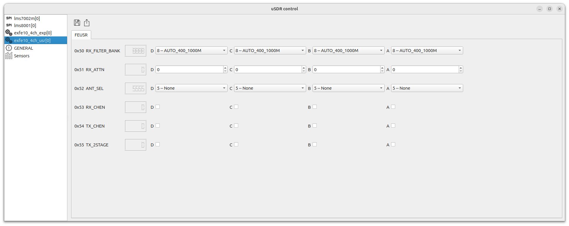
FE control registers
RX_FILTER_BANK/A- RX filter bank selector for channel AOptions:
FILT_50_1000M- RX filter 50-1000 MHzFILT_1000_2000M- RX filter 1000-2000 MHzFILT_2000_3500M- RX filter 2000-3500 MHzFILT_2500_5000M- RX filter 2500-5000 MHzFILT_3500_7100M- RX filter 3500-7100 MHzAUTO_50_1000M- Sets filter automatically by LO frequency / Shows selected filter when in AUTO modeAUTO_1000_2000M- Sets filter automatically by LO frequency / Shows selected filter when in AUTO modeAUTO_2000_3500M- Sets filter automatically by LO frequency / Shows selected filter when in AUTO modeAUTO_2500_5000M- Sets filter automatically by LO frequency / Shows selected filter when in AUTO modeAUTO_3500_7100M- Sets filter automatically by LO frequency / Shows selected filter when in AUTO mode
RX_FILTER_BANK/B- RX filter bank selector for channel BOptions: same as channel A
RX_FILTER_BANK/C- RX filter bank selector for channel COptions: same as channel A
RX_FILTER_BANK/D- RX filter bank selector for channel DOptions: same as channel A
RX_ATTN/A- RX attenuator setting (dB) for channel A
RX_ATTN/B- RX attenuator setting (dB) for channel B
RX_ATTN/C- RX attenuator setting (dB) for channel C
RX_ATTN/D- RX attenuator setting (dB) for channel D
ANT_SEL/A- Antenna path selector for channel AOptions:
RX_TO_RX_AND_TX_TO_TRX- RX to RX path and TX to TRX pathRX_TO_TRX_AND_TX_TERM- RX to TRX path and TX terminatedRX_TO_RX_AND_TX_TERM- RX to RX path and TX terminatedRX_TX_LOOPBACK- RX to TX loopbackTDD_DRIVEN_AUTO- Automatic TDD mode
ANT_SEL/B- Antenna path selector for channel BOptions: same as channel A
ANT_SEL/C- Antenna path selector for channel COptions: same as channel A
ANT_SEL/D- Antenna path selector for channel DOptions: same as channel A
RX_CHEN/A- Enable RX channel A
RX_CHEN/B- Enable RX channel B
RX_CHEN/C- Enable RX channel C
RX_CHEN/D- Enable RX channel D
TX_CHEN/A- Enable TX channel A
TX_CHEN/B- Enable TX channel B
TX_CHEN/C- Enable TX channel C
TX_CHEN/D- Enable TX channel D
TX_2STAGE/A- Enable TX 2nd stage for channel A
TX_2STAGE/B- Enable TX 2nd stage for channel B
TX_2STAGE/C- Enable TX 2nd stage for channel C
TX_2STAGE/D- Enable TX 2nd stage for channel D
exfe10_4ch_exp
This section describes the low level control register map for the FE front-end. Using this page, you can control each hardware component directly.
Warning
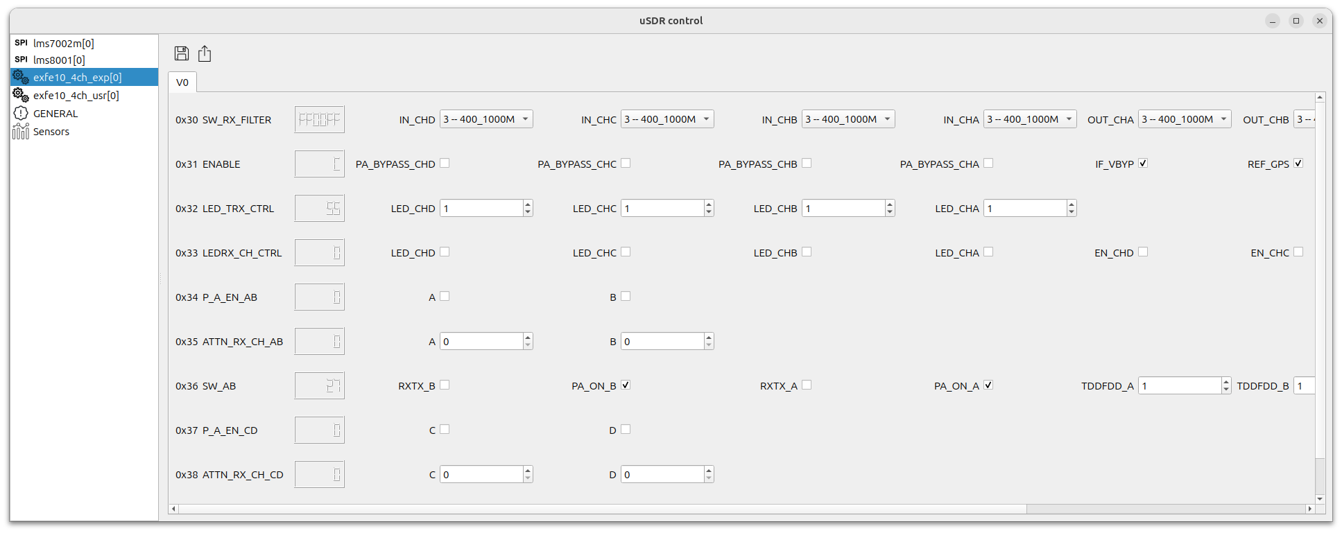
FE control lowlevel registers
SW_RX_FILTER/IN_CHA- RX IN filters switch for Channel AOptions:
MUTE0- Mute / Disconnected50_1000M- Input filter bank switch to filter 50-1000 MHz1000_2000M- Input filter bank switch to filter 1000-2000 MHz2000_3500M- Input filter bank switch to filter 2000-3500 MHz2500_5000M- Input filter bank switch to filter 2500-5000 MHz3500_7100M- Input filter bank switch to filter 3500-7100 MHzMUTE1- Mute / DisconnectedMUTE2- Mute / Disconnected
SW_RX_FILTER/OUT_CHA- RX OUT filters switch for Channel AOptions:
MUTE0- Mute / Disconnected50_1000M- Output filter bank switch to filter 50-1000 MHz1000_2000M- Output filter bank switch to filter 1000-2000 MHz2000_3500M- Output filter bank switch to filter 2000-3500 MHz2500_5000M- Output filter bank switch to filter 2500-5000 MHz3500_7100M- Output filter bank switch to filter 3500-7100 MHzMUTE1- Mute / DisconnectedMUTE2- Mute / Disconnected
SW_RX_FILTER/IN_CHB- RX IN filters switch for Channel BOptions: same as Channel A
SW_RX_FILTER/OUT_CHB- RX OUT filters switch for Channel BOptions: same as Channel A
SW_RX_FILTER/IN_CHC- RX IN filters switch for Channel COptions: same as Channel A
SW_RX_FILTER/OUT_CHC- RX OUT filters switch for Channel COptions: same as Channel A
SW_RX_FILTER/IN_CHD- RX IN filters switch for Channel DOptions: same as Channel A
SW_RX_FILTER/OUT_CHD- RX OUT filters switch for Channel DOptions: same as Channel A
ENABLE/IF_VBYP- IF bypass control
ENABLE/REF_GPS- Enable GPS module
ENABLE/P8V_TX- Enable +8V power supply for TX amps
ENABLE/P6V_RX- Enable +6V power supply for RX amps
ENABLE/PA_BYPASS_CHD- Stage-2 PA bypass, channel D
ENABLE/PA_BYPASS_CHC- Stage-2 PA bypass, channel C
ENABLE/PA_BYPASS_CHB- Stage-2 PA bypass, channel B
ENABLE/PA_BYPASS_CHA- Stage-2 PA bypass, channel A
LED_TRX_CTRL/LED_CHA- LED TX/RX control for Channel A
LED_TRX_CTRL/LED_CHB- LED TX/RX control for Channel B
LED_TRX_CTRL/LED_CHC- LED TX/RX control for Channel C
LED_TRX_CTRL/LED_CHD- LED TX/RX control for Channel D
LEDRX_CH_CTRL/EN_CHA- Enable LED CHA
LEDRX_CH_CTRL/EN_CHB- Enable LED CHB
LEDRX_CH_CTRL/EN_CHC- Enable LED CHC
LEDRX_CH_CTRL/EN_CHD- Enable LED CHD
LEDRX_CH_CTRL/LED_CHA- LED CHA indicator
LEDRX_CH_CTRL/LED_CHB- LED CHB indicator
LEDRX_CH_CTRL/LED_CHC- LED CHC indicator
LEDRX_CH_CTRL/LED_CHD- LED CHD indicator
P_A_EN_AB/B- Enable CHB (PA enable AB)
P_A_EN_AB/A- Enable CHA (PA enable AB)
ATTN_RX_CH_AB/B- Attenuator CHB
ATTN_RX_CH_AB/A- Attenuator CHA
SW_AB/TDDFDD_A- TDD/FDD control bits (A)
SW_AB/TDDFDD_B- TDD/FDD control bits (B)
SW_AB/PA_ON_A- PA on control for A
SW_AB/PA_ON_B- PA on control for B
SW_AB/RXTX_A- RX/TX switch control for A
SW_AB/RXTX_B- RX/TX switch control for B
P_A_EN_CD/D- Enable CHD (PA enable CD)
P_A_EN_CD/C- Enable CHC (PA enable CD)
ATTN_RX_CH_CD/D- Attenuator CHD
ATTN_RX_CH_CD/C- Attenuator CHC
SW_CD/TDDFDD_C- TDD/FDD control bits (C)
SW_CD/TDDFDD_D- TDD/FDD control bits (D)
SW_CD/PA_ON_C- PA on control for C
SW_CD/PA_ON_D- PA on control for D
SW_CD/RXTX_C- RX/TX switch control for C
SW_CD/RXTX_D- RX/TX switch control for D
Measurements
This section contains measurements for the RF paths on the FE board.
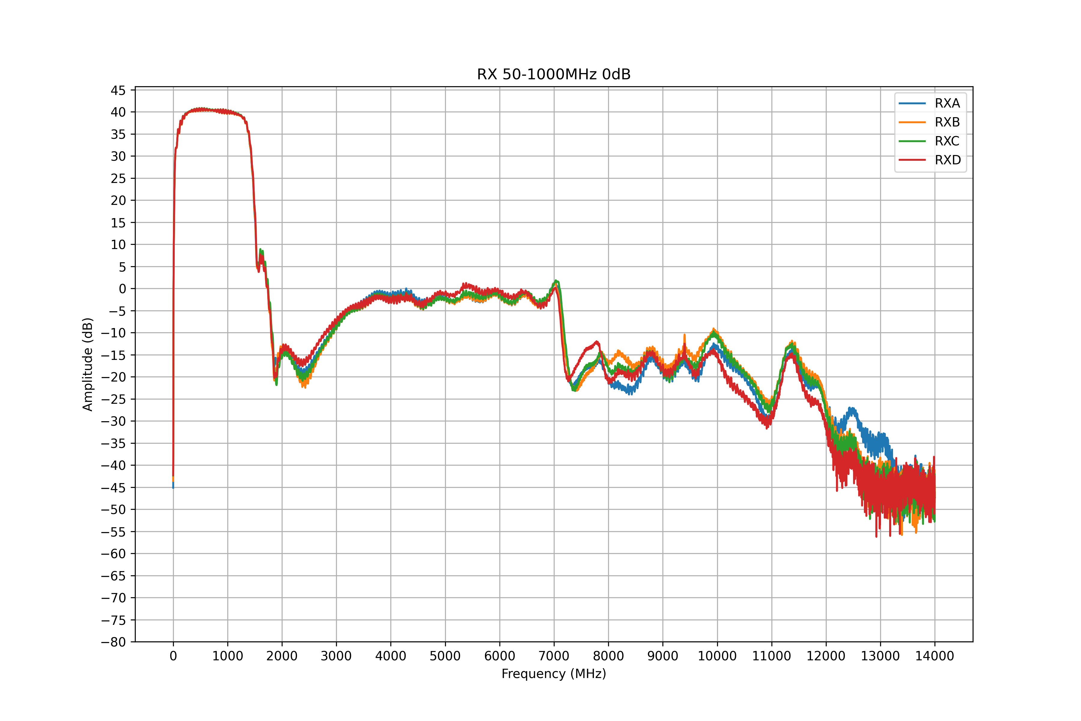
Parameters of RX path with 50-1000MHz filter at 0dB attenuation
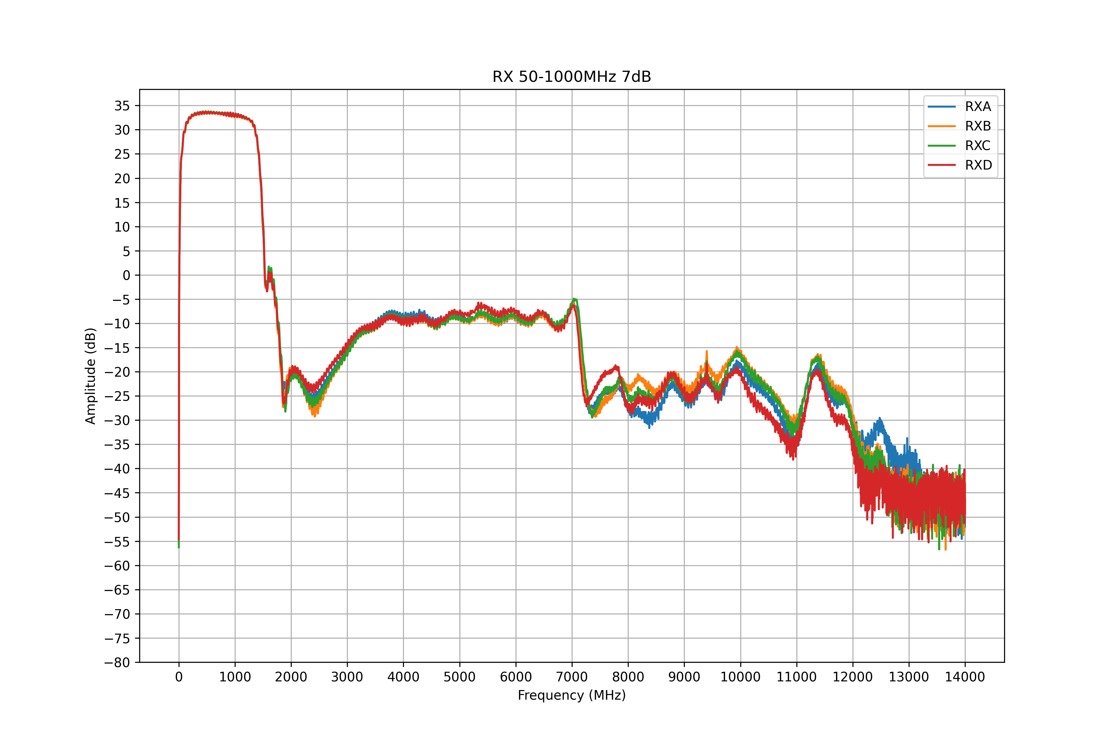
Parameters of RX path with 50-1000MHz filter at 7dB attenuation
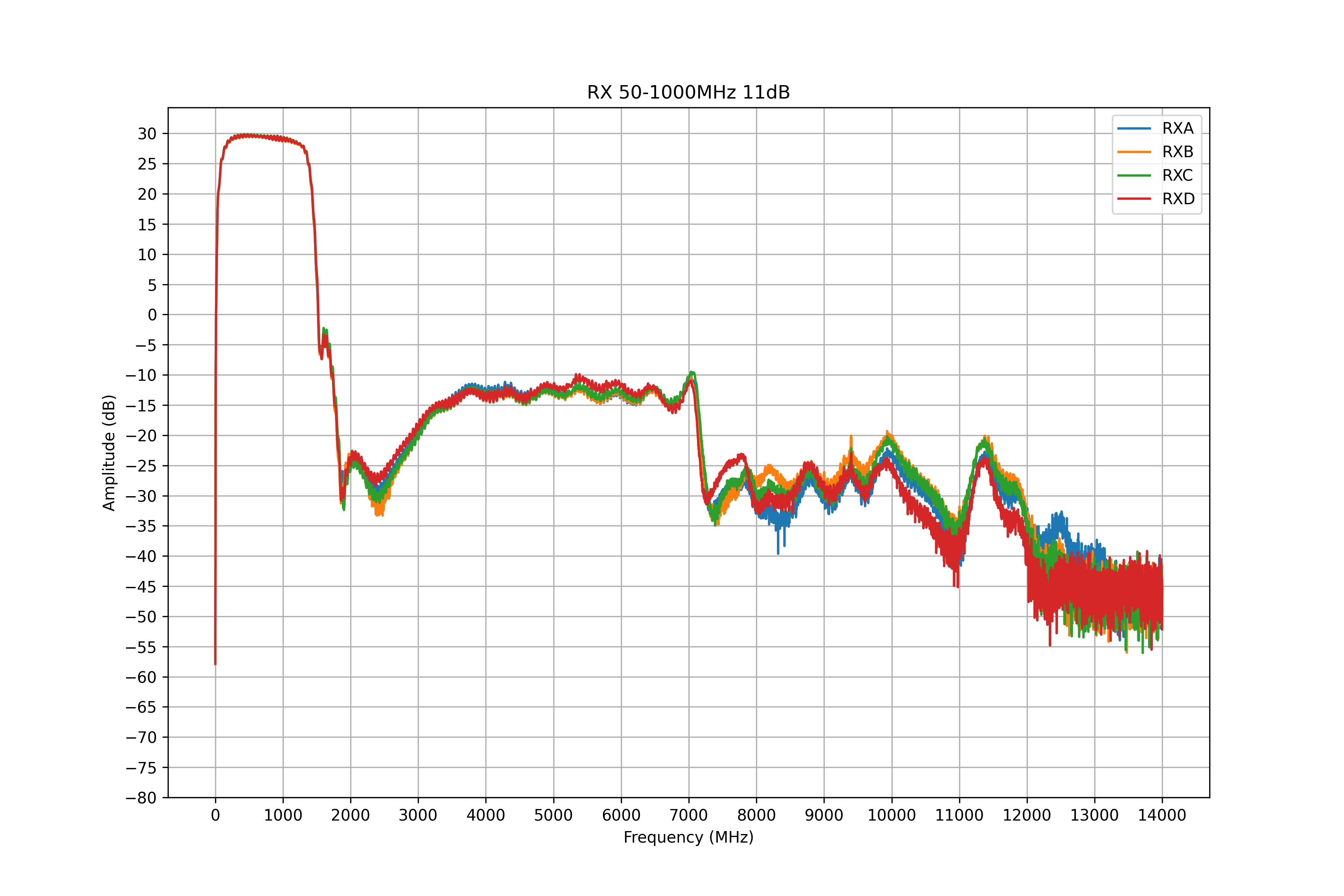
Parameters of RX path with 50-1000MHz filter at 11dB attenuation
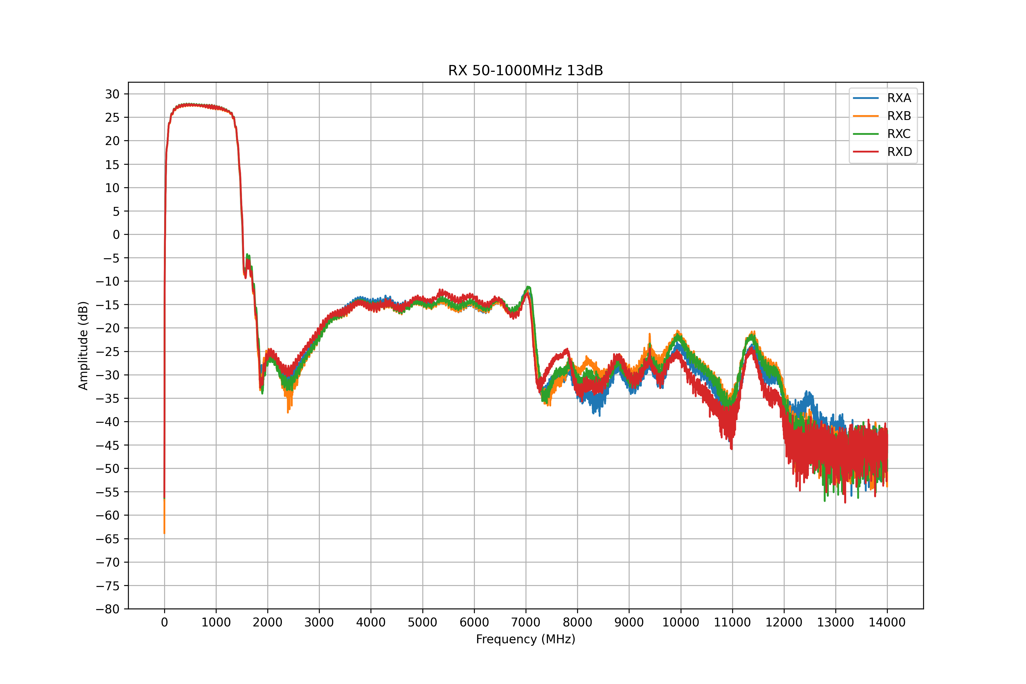
Parameters of RX path with 50-1000MHz filter at 13dB attenuation
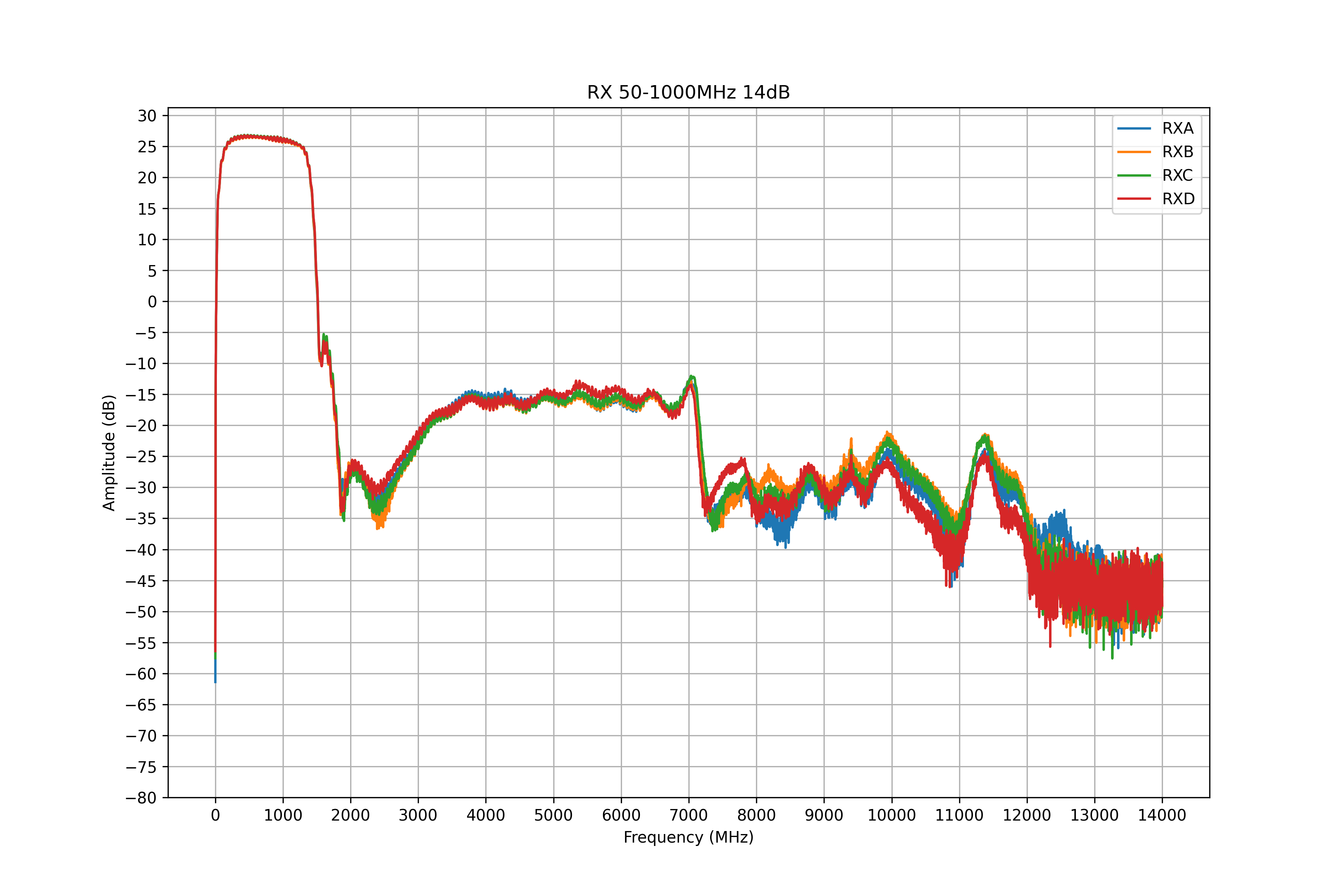
Parameters of RX path with 50-1000MHz filter at 14dB attenuation

Parameters of RX path with 50-1000MHz filter at 15dB attenuation
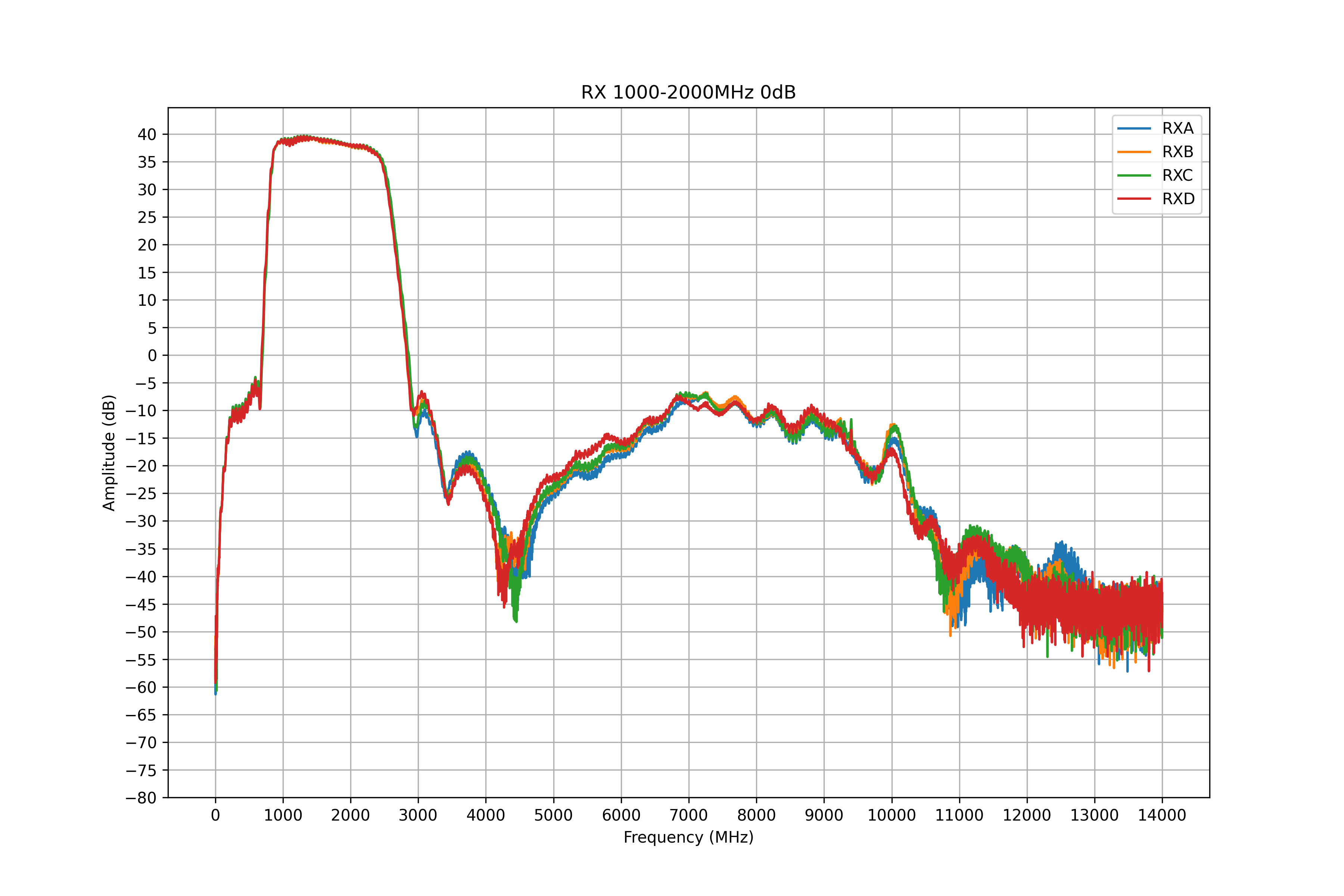
Parameters of RX path with 1000-2000MHz filter
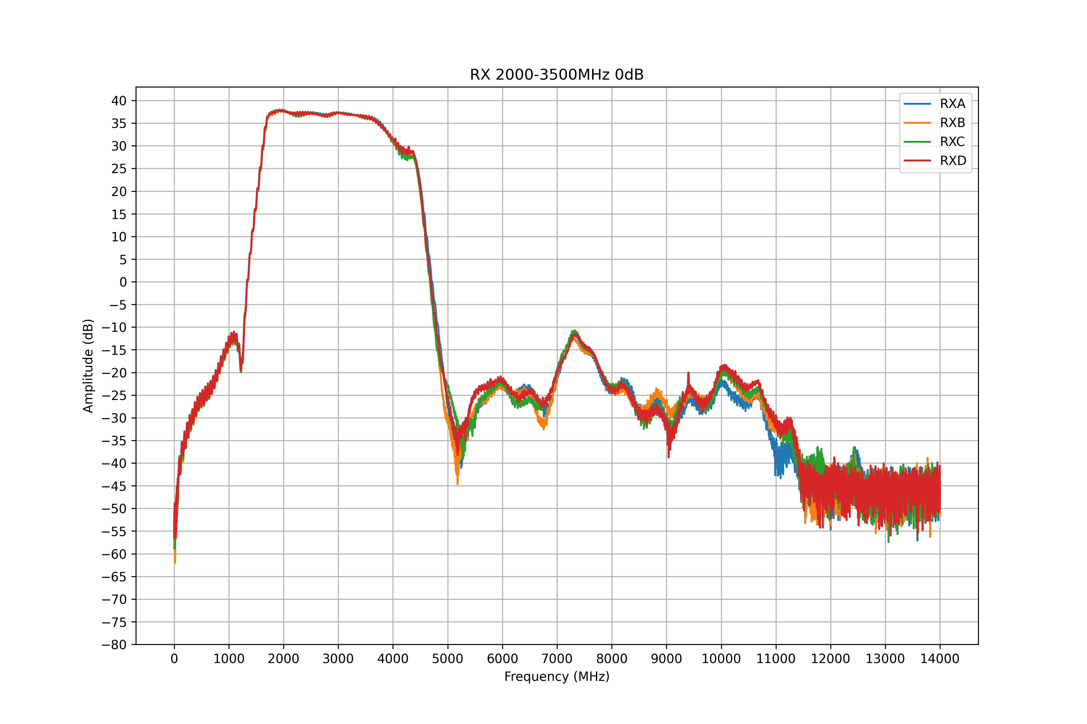
Parameters of RX path with 2000-3500MHz filter
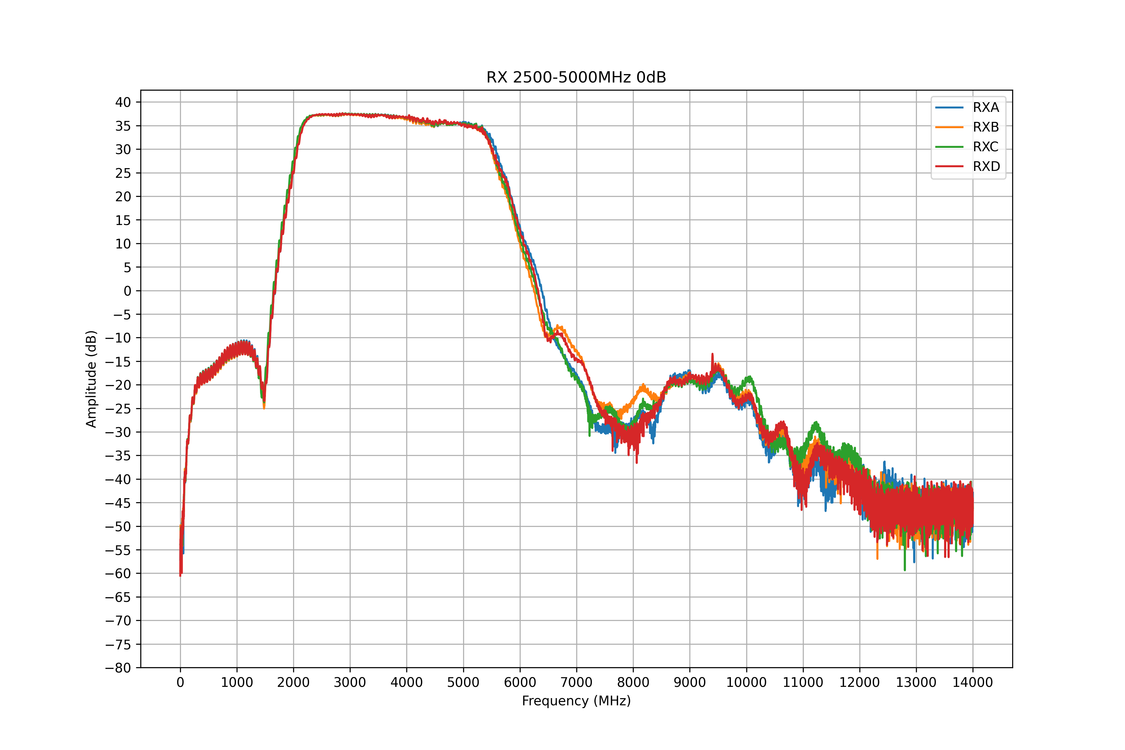
Parameters of RX path with 2500-5000MHz filter
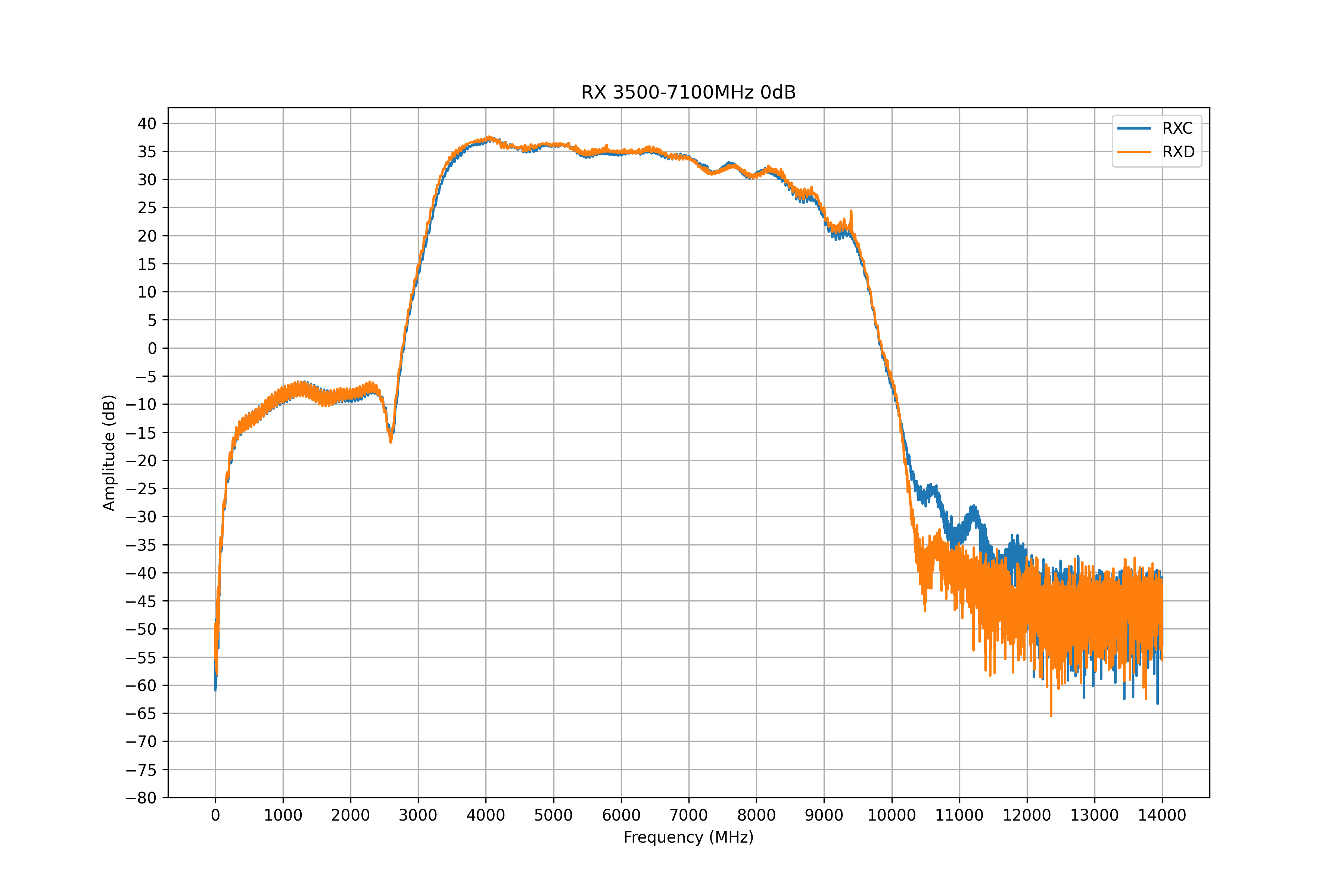
Parameters of RX path with 3500-7100MHz filter
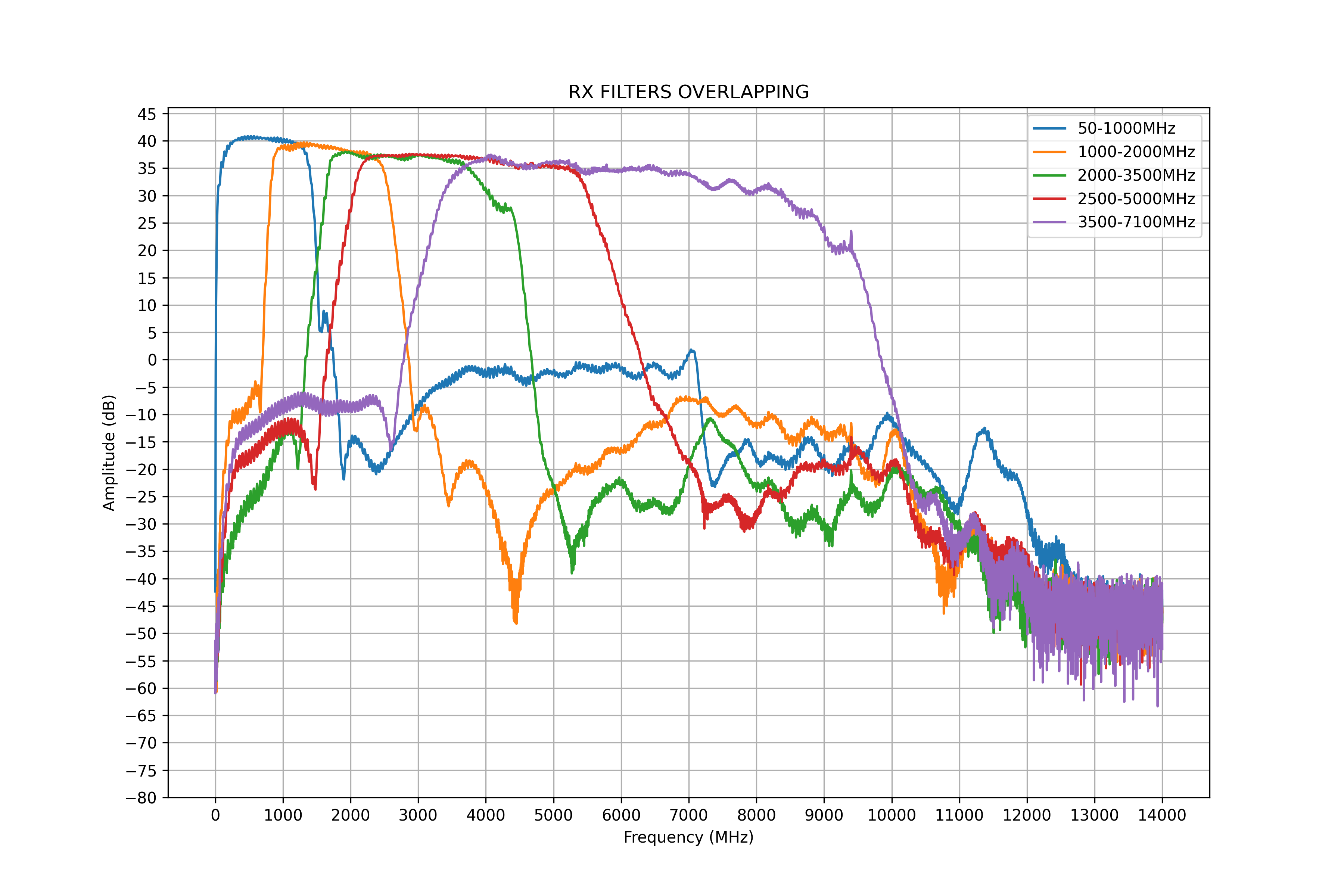
Filters overlapping characteristics
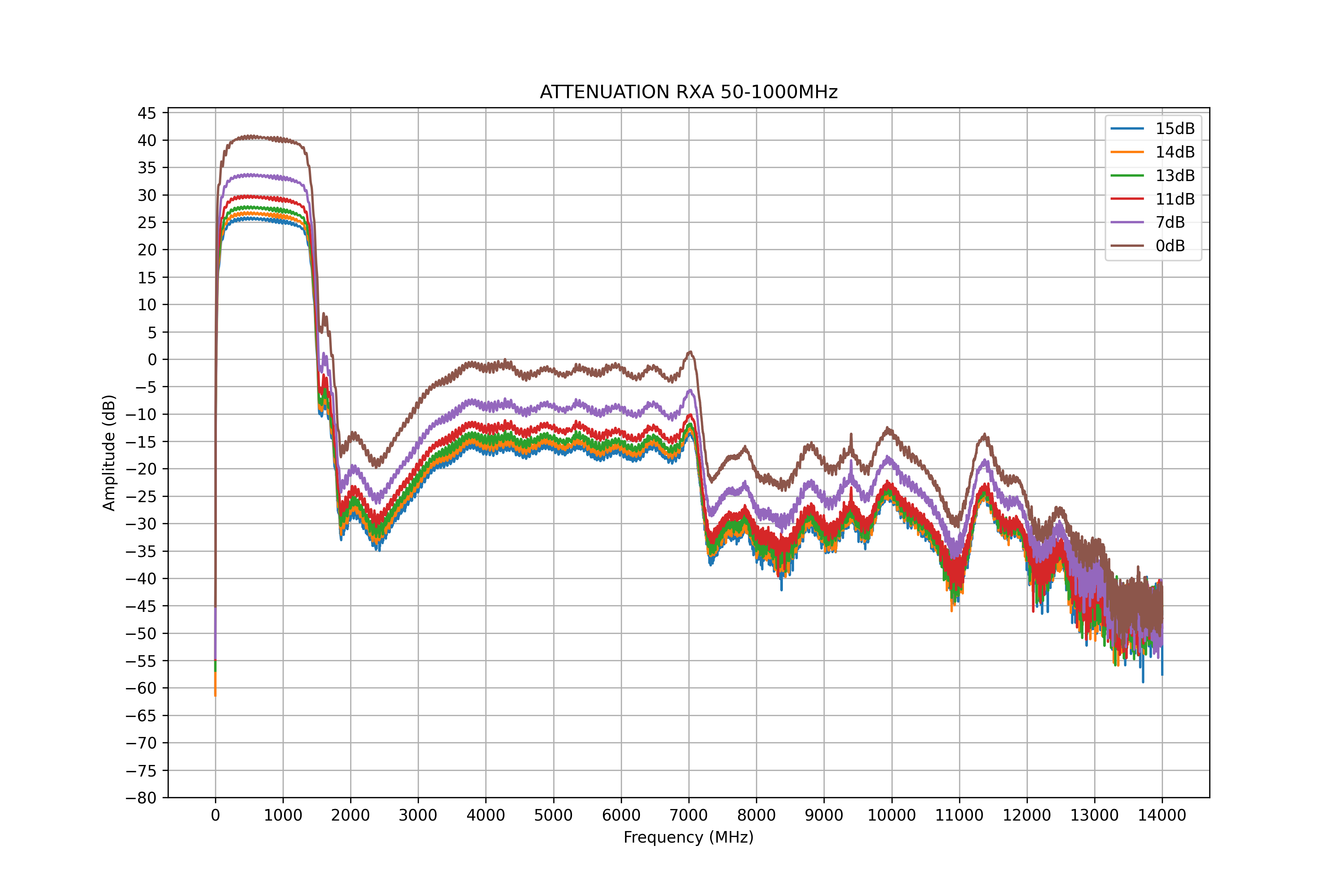
Attenuation characteristics for RX channel A with 50-1000MHz filter

Attenuation characteristics for RX channel B with 50-1000MHz filter
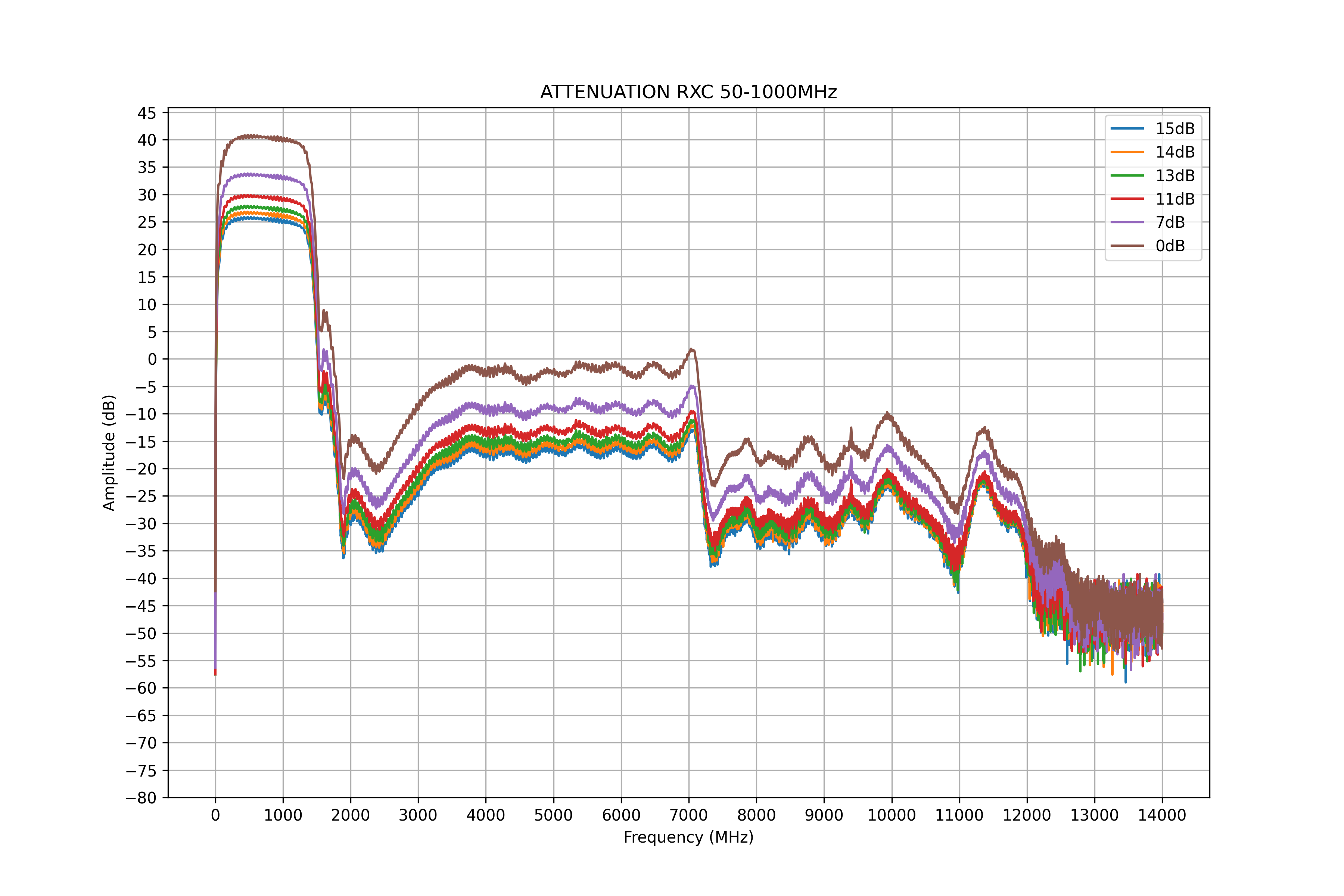
Attenuation characteristics for RX channel C with 50-1000MHz filter
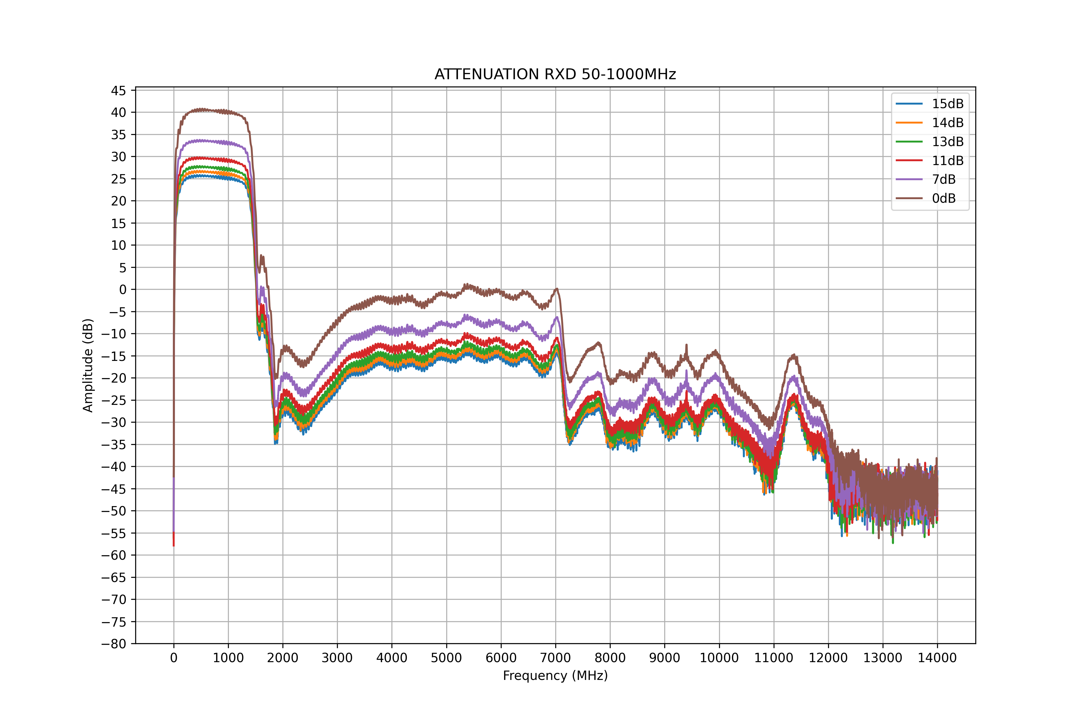
Attenuation characteristics for RX channel D with 50-1000MHz filter
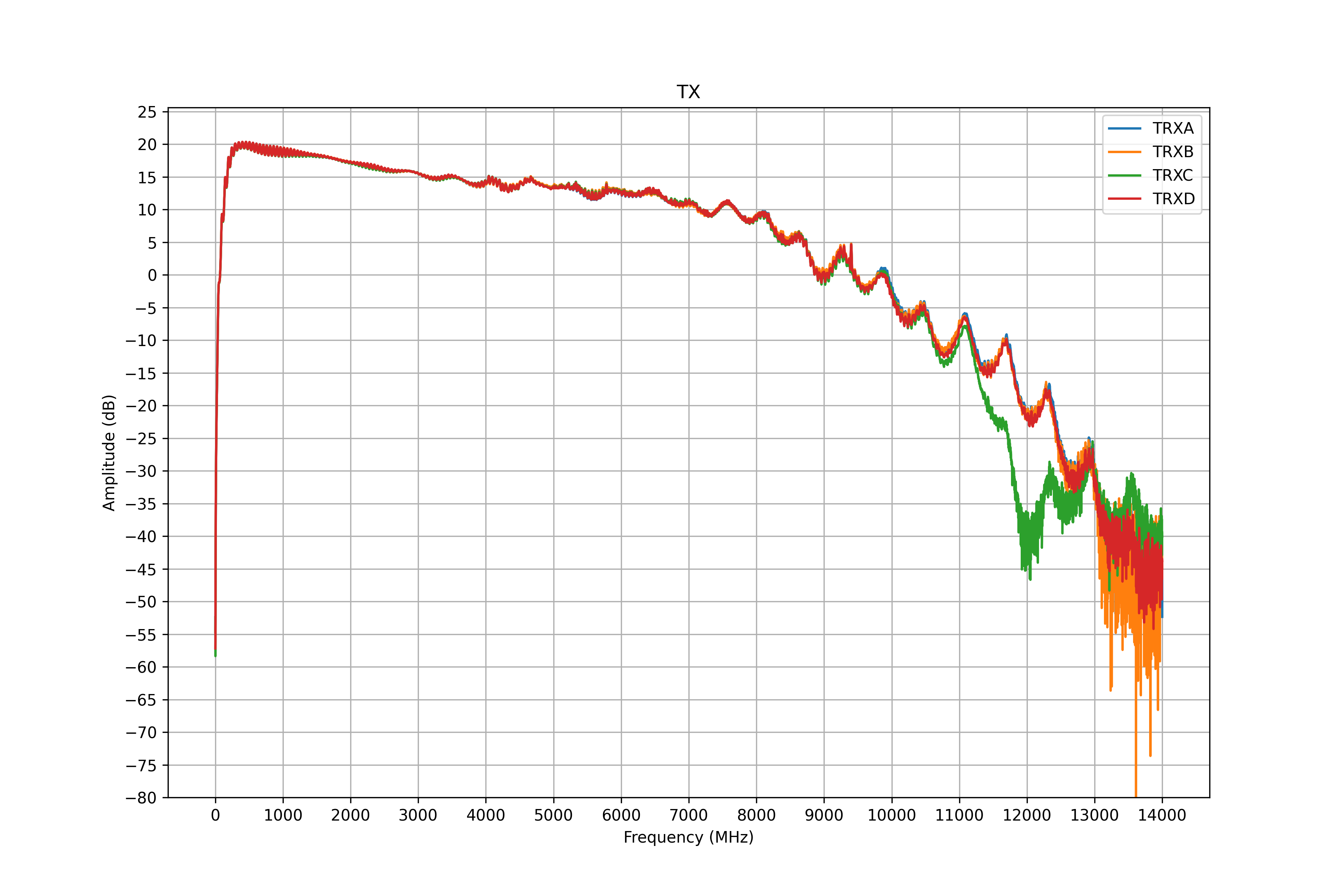
Parameters of TX path
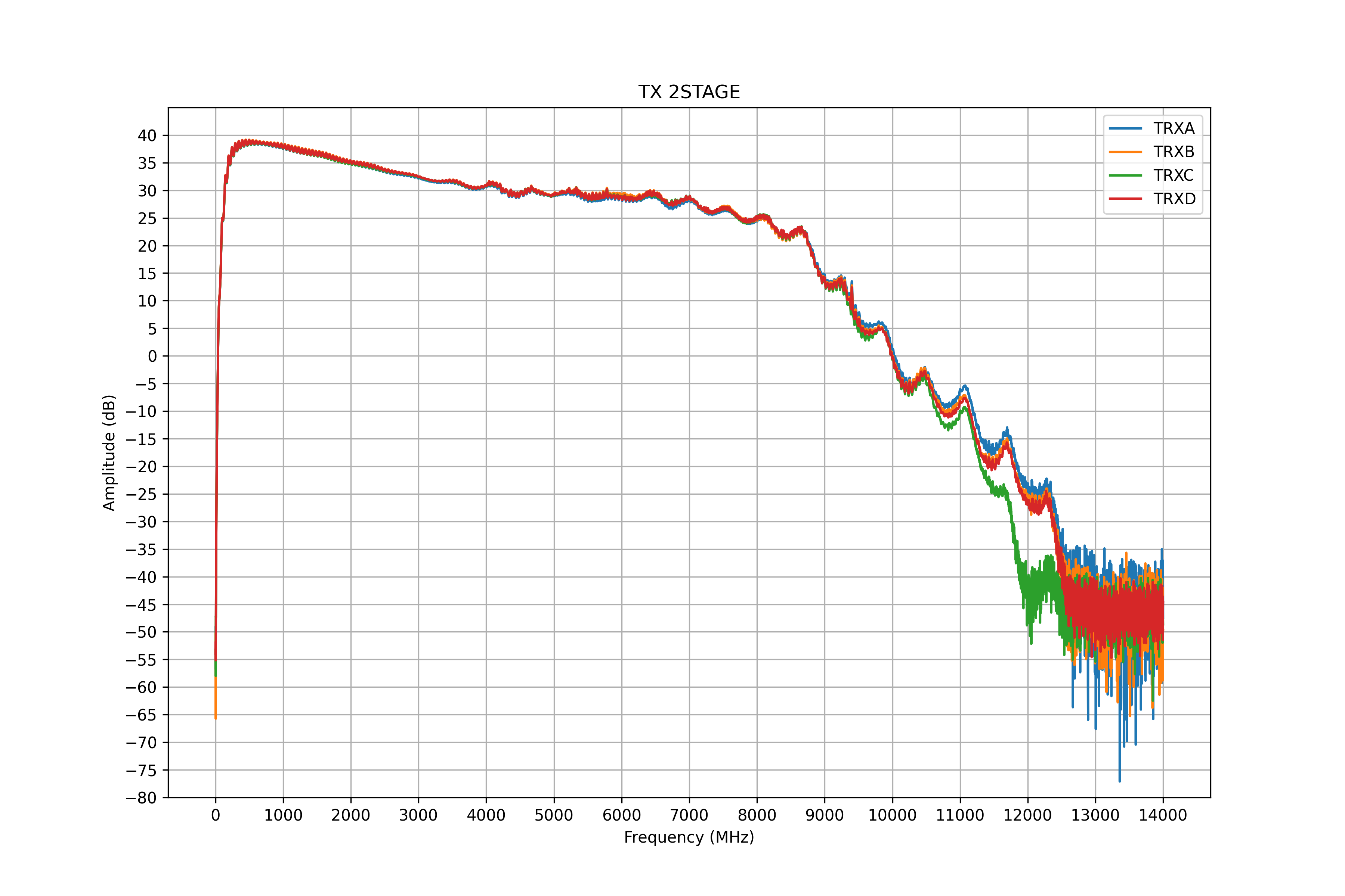
Parameters of TX path with 2-stage PA
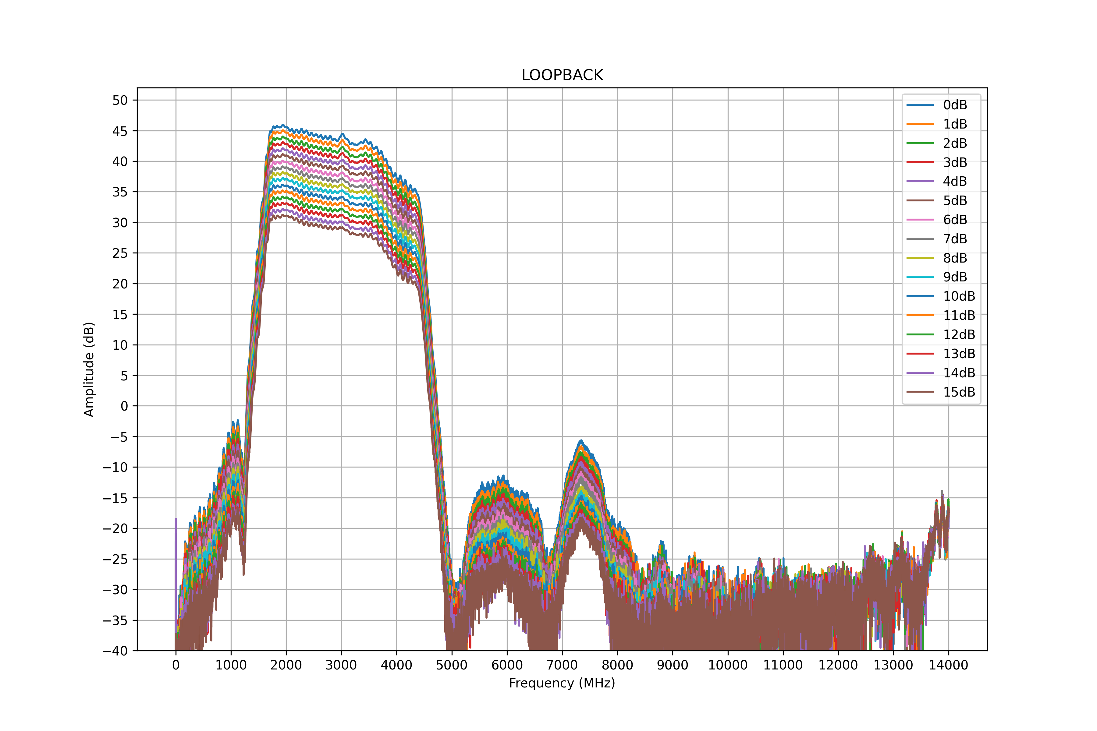
Parameters of LOOPBACK path with different attenuation levels
Software
Caution
feature_pe_sync branch.In order to use FE, you can use the usdr_dm_create utility to receive or transmit data.
The following example creates a raw IQ data file with a sample rate of 10 MSamples per second per channel, a center frequency of 1700 MHz, using all 4 RX channels:
usdr_dm_create -D -r10e6 -l3 -e1700e6 -c -1 -f output.raw
The software stack supports the SoapySDR interface, so you can use any compatible application.